Titanium Anode for PCB Gold Plating: Key Technologies for Uniform Coating
A PCB fabrication plant running ENIG on HDI boards with 0.1 mm via pitch pulls its first inspection lot and finds gold deposit thickness ranging from 0.08 μm at panel center to 0.14 μm at panel edges — a 75% variation against a specification calling for 0.05–0.10 μm across the full panel. Bath chemistry checks come back clean. Gold concentration, pH, temperature, and additive levels are all within range. The process engineer pulls the anode rack and finds the answer immediately: the platinum-coated titanium anodes are 40 mm narrower than the panel width on each side, and the anode-to-cathode spacing is 180 mm — far outside the recommended envelope for the current density being run. This is not a chemistry problem. It is an anode geometry problem, and it is the most common root cause of gold plating non-uniformity on production PCB lines.
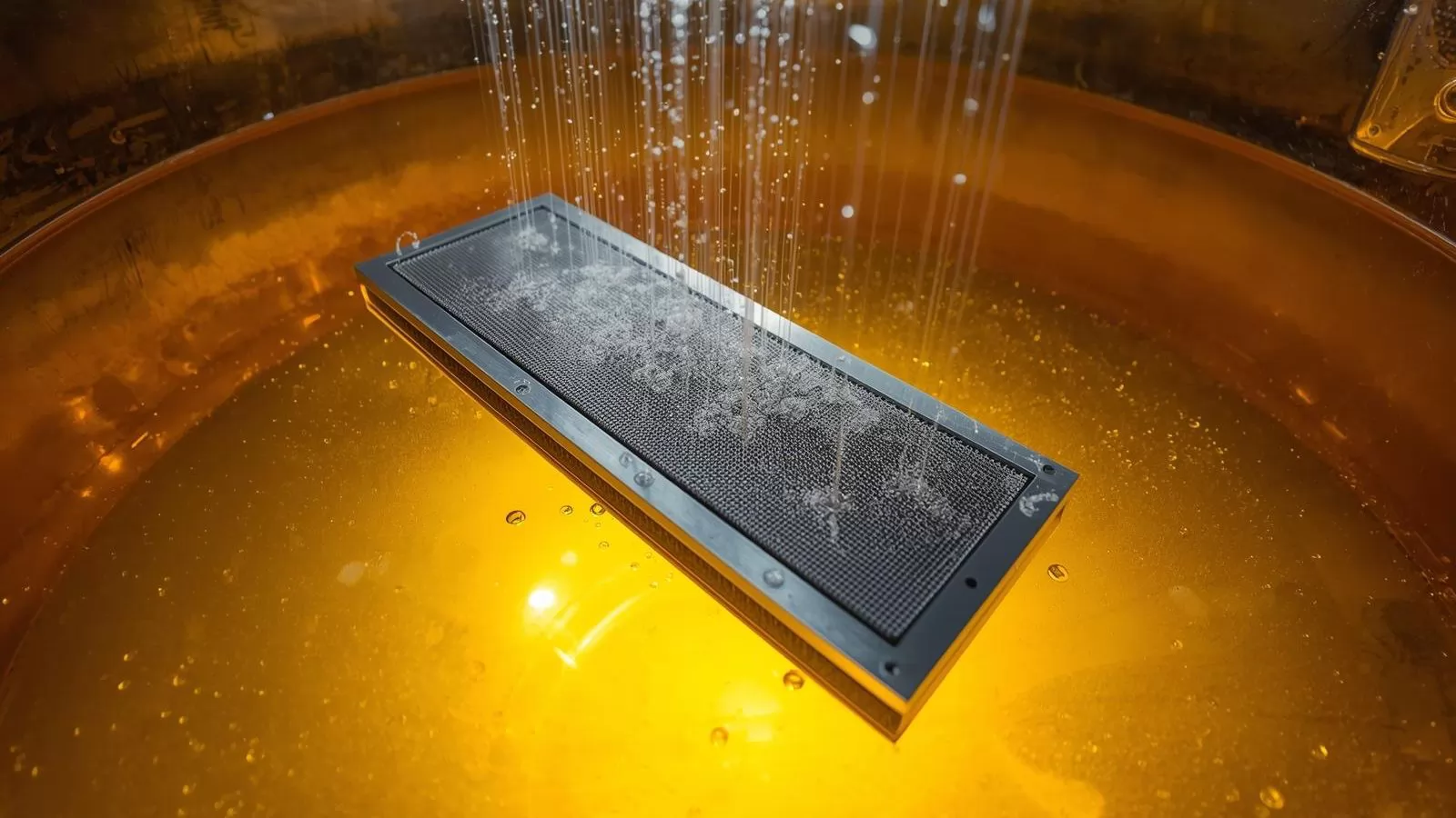
Achieving uniform gold coating on PCB gold plating lines requires titanium insoluble anodes — with platinum or MMO coatings — as the engineering standard, because only insoluble anodes decouple bath gold concentration from anode dissolution rate. Anode geometry and platinum loading are the two primary variables that control current distribution uniformity across the board panel, while coating type determines long-term bath chemistry stability, contamination risk, and anode service life across acid, neutral, and alkaline gold bath chemistries.

Why PCB Gold Plating Demands Insoluble Anodes
The shift from soluble gold anodes to insoluble titanium anodes in PCB gold electroplating was not driven by cost — soluble gold anodes are cheaper to procure. It was driven by two process failures that soluble anodes produce reliably at production scale, and that insoluble anodes eliminate structurally.
Failure Mode 1: Bath Gold Concentration Drift from Non-Uniform Dissolution
A soluble gold anode dissolves during electrolysis — that is its function. But dissolution rate is not uniform across the anode surface. High-current-density zones at anode edges and corners dissolve faster than the anode center, which means the anode geometry changes progressively during its service life. As geometry changes, current distribution shifts, bath gold concentration rises and falls in local zones, and deposit thickness across the panel becomes unpredictable. On a production line running 500×600 mm rigid PCB panels to a gold specification of ±15% thickness tolerance, this variability routinely produces out-of-spec boards within the first 200 A·h of bath loading.
Failure Mode 2: Bath Contamination from Anode Sludge and Co-Dissolved Metals
Soluble gold anodes are never 100% pure gold. Co-dissolved base metal impurities — copper, silver, and trace alloying elements — enter the bath with each dissolution cycle. Anode sludge accumulates at the bottom of the plating cell, and fine sludge particles can co-deposit with gold onto the PCB surface. For standard PCB connector plating, this degrades gold deposit hardness and appearance. For semiconductor packaging PCB applications where wire-bondable gold is specified, co-deposited impurities above threshold concentrations cause wire bond pull-test failures — a quality escape that costs significantly more than the scrap value of the boards involved.
How Insoluble Titanium Anodes Eliminate Both Failure Modes
Platinum-coated titanium anodes and MMO coated titanium anodes are insoluble — the anodic reaction that occurs at their surface is oxygen evolution (OER), not metal dissolution. The platinum or oxide coating catalyzes the oxidation of water to O₂ gas; the anode itself does not dissolve and does not change geometry during service. This has two direct process consequences:
- Bath gold concentration is controlled entirely by chemical replenishment — gold salt is added to the bath at a metered rate calibrated to the plating current draw. There is no dissolution variable. Concentration stays within specification indefinitely if replenishment is managed correctly.
- Zero contamination from the anode — the platinum coating specified by JH Ti Anode carries 99.99% Pt purity. No base metal ions, no sludge, no particle co-deposition. For aerospace and semiconductor packaging PCB specifications requiring wire-bondable gold purity, this is the only anode type that passes the contamination requirements of the specification.
Why platinum rather than MMO for gold plating baths specifically? MMO coatings (Ru–Ir–Ti) are excellent for chloride-bearing electrolytes and industrial wastewater treatment — see the site's coverage of titanium anode applications in industrial wastewater treatment for those applications. In gold sulfite plating baths, the concern is coating-derived ion contamination: ruthenium and iridium ions, even at sub-ppm concentrations, can alter gold deposit crystallography and affect bondability. Platinum at 99.99% purity introduces no such risk, which is why it is the preferred specification for gold plating baths where deposit purity is the defining quality criterion.
Current Distribution Physics — How Anode Geometry Controls Gold Deposit Uniformity
Every gold plating uniformity problem has a current distribution root cause. Understanding which of the three current distribution regimes is controlling your process determines which corrective action will work — and which changes to bath chemistry, rectifier settings, or additives will have no effect at all.
Primary Current Distribution — Geometry Dominates
Primary current distribution is determined by cell geometry alone: the shape and position of the anode relative to the cathode (PCB panel), and the anode-to-cathode spacing. It assumes zero solution resistance and zero electrode kinetic resistance — a useful theoretical limit that describes the behavior of plating cells operating at very low current density (below 0.5 A/dm² for most gold bath chemistries).
At primary distribution conditions, the edge effect is severe. Current lines concentrate at the geometric edges and corners of the panel because those points are closest to the anode and present the lowest resistance path. A panel plated under primary distribution control with a flat plate anode will consistently show 30–50% higher deposit thickness at panel corners than at the geometric center — independent of bath chemistry or additive formulation. The corrective action at this level is always geometric: extend anode width to match or exceed board width, reduce anode-to-cathode spacing, or use conformally shaped anodes that follow the board perimeter to reduce the edge-to-center current ratio.
Secondary Current Distribution — Solution Resistance and Electrode Kinetics
Secondary current distribution accounts for solution resistance and electrode kinetic effects. As bath conductivity increases (higher gold sulfite concentration, higher supporting electrolyte loading), solution resistance decreases and the distribution shifts away from primary geometry control toward a more uniform pattern. This is why bath conductivity is a process lever for uniformity — but it is a lever with diminishing returns. You cannot correct a primary geometry problem with conductivity adjustments alone.
The electrode kinetics term in secondary distribution is where anode coating selection has a measurable effect on uniformity. Platinum-coated titanium anodes have lower OER overpotential than bare titanium — the platinum surface catalyzes the oxygen evolution reaction at a lower activation energy. This means more of the applied cell voltage drives ionic current through the solution rather than being consumed at the anode surface. The practical effect is a modest improvement in secondary distribution uniformity at equivalent current density, particularly relevant in the 0.5–2.0 A/dm² operating range typical of PCB soft gold and ENIG plating.
Tertiary Current Distribution — Mass Transfer at High Current Density
At current densities above 2 A/dm², mass transfer of gold ions to the cathode surface becomes the rate-limiting step, and tertiary current distribution controls deposit uniformity. In this regime, the geometry of the anode has a direct effect on electrolyte convection in the cell — which in turn controls how uniformly gold ions are replenished at the board surface.
Mesh anodes, by allowing electrolyte to flow through the anode structure, promote convection across the face of the PCB panel. This reduces concentration polarization at the board surface and improves deposit uniformity at high current density. Solid plate anodes create a stagnant electrolyte zone between the anode back-face and the cell wall — this does not directly affect the plating surface, but it reduces the total convective mixing in the cell. For high-CD applications (hard gold connector plating, pulse plating at peak densities above 5 A/dm²), specify mesh form anodes. For low-CD applications (ENIG, soft gold rack plating at 0.3–1.0 A/dm²), plate anodes with forced electrolyte flow are acceptable.
Practical Parameters for Anode Specification
| Parameter | Rack Plating (Soft Gold / ENIG) | Hard Gold / Selective Plating | Pulse Plating (HDI) |
|---|---|---|---|
| Anode-cathode spacing | 80–150 mm | 50–100 mm | 30–80 mm |
| Current density | 0.3–1.5 A/dm² | 1–5 A/dm² | Peak 5–20 A/dm²; avg 0.5–2 A/dm² |
| Platinum loading | 2–5 g/m² | 5–15 g/m² | 5–10 g/m² |
| Preferred anode form | Plate or mesh | Tube or rod (selective); mesh (rack) | Mesh |
| Dominant distribution regime | Primary / secondary | Secondary / tertiary | Tertiary (peak); secondary (average) |

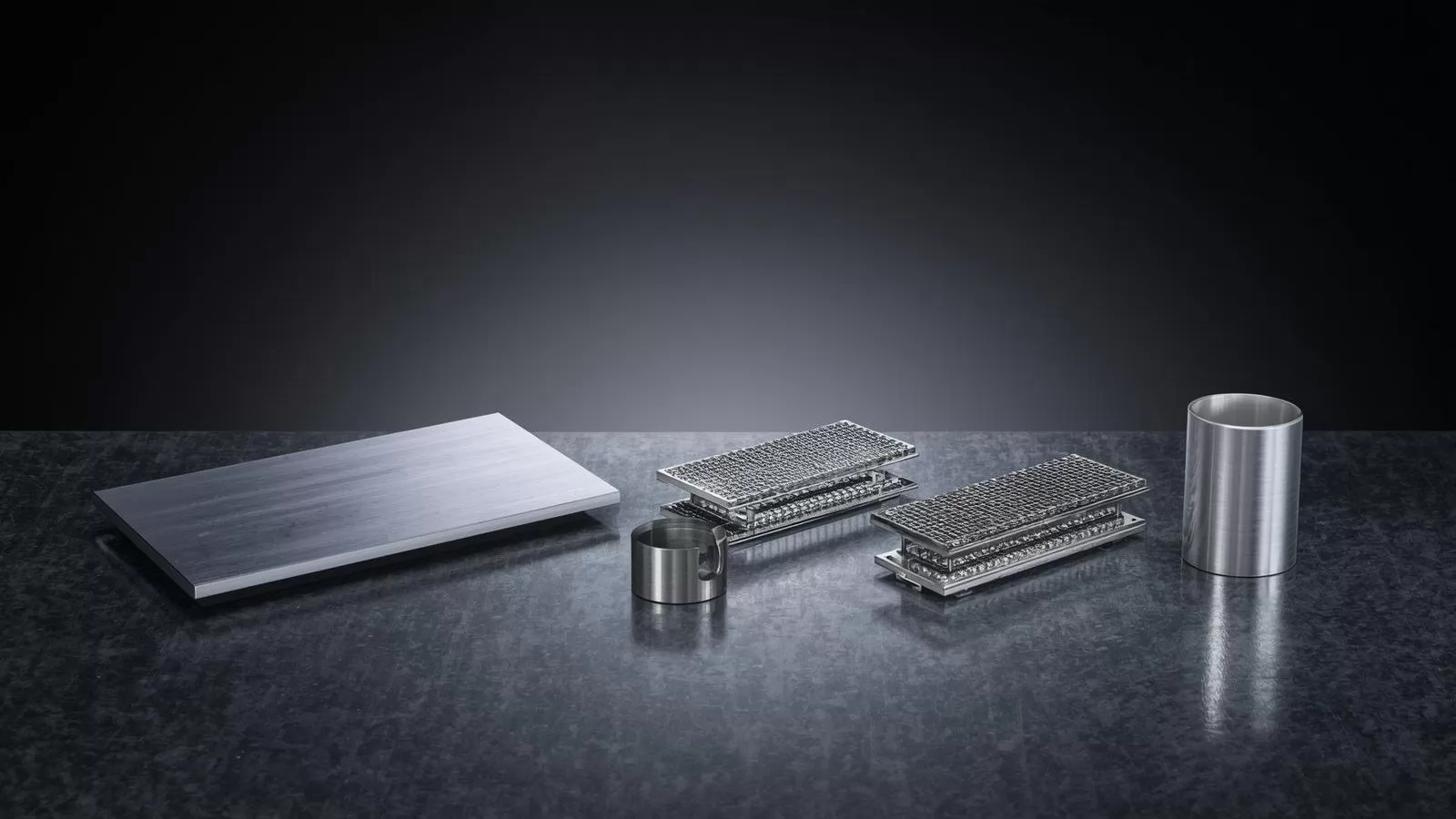
Anode Form Selection Guide — Matching Geometry to PCB Gold Plating Process Type
The anode form factor is not interchangeable across PCB gold plating process types. Each process type has a different panel geometry, current density requirement, and mass transfer regime — and each demands a specific anode form to achieve the deposit uniformity the process specification requires.
Process Type 1 — Rack Plating (ENIG / Soft Gold)
Board type: Rigid PCB panels, typically 500×600 mm production format.
Recommended anode form: Flat plate or expanded mesh, full-panel width or wider. Anode width must match or exceed panel width — undersized anodes are the most common cause of edge-starvation non-uniformity on ENIG lines.
Platinum loading: 2–5 g/m². At 0.3–1.0 A/dm², coating wear rate is low — this loading provides multi-year service life under normal ENIG production conditions.
Current density: 0.3–1.0 A/dm².
Anode-cathode spacing: 80–150 mm.
Key constraint: Anode dimensional stability at full panel width is non-negotiable. Graphite warps under thermal cycling and current load, progressively increasing anode-cathode spacing non-uniformity across the panel width. Titanium plate and mesh maintain flatness. Specify hardware electroplating titanium anodes in plate or mesh form for all ENIG rack plating installations.
Process Type 2 — Reel-to-Reel Selective Gold Plating
Board type: Flexible PCB strip, connector edge fingers, reel-format substrates.
Recommended anode form: Narrow tubular or rod anode, positioned precisely above the plating window with a mask defining the selective plating area.
Platinum loading: 5–15 g/m². Reel-to-reel selective plating operates at high current density — coating wear is proportionally higher, and platinum loading must be specified to meet the target service interval between anode replacement cycles.
Current density: 2–8 A/dm².
Anode-cathode spacing: 10–40 mm (tight tolerances required to maintain plating window definition).
Key constraint: Reel-to-reel line speed is matched to current density to hit target deposit thickness. If the anode geometry drifts — due to dimensional instability or wear — the current delivered per unit area of strip changes, and deposit thickness moves out of specification at reel speed. Titanium rod and tube anodes maintain their cross-sectional geometry throughout service life. Use platinum-coated titanium anodes in tube or rod form, custom-sized to the plating window dimensions.
Process Type 3 — Barrel Plating (Small PCB Components)
Board type: PCB edge connectors, small terminals, through-hole components requiring gold finish.
Recommended anode form: Rod or wire anodes arranged around the barrel periphery.
Platinum loading: 2–8 g/m² depending on operating current density and target service interval.
Current density: 0.5–2 A/dm².
Key constraint: Barrel plating subjects anodes to mechanical agitation — the barrel rotates through the electrolyte and can cause intermittent mechanical contact between barrel contents and anode rods. Titanium substrate provides the mechanical strength to tolerate this without deformation. Specify rod form with adequate wall thickness for the barrel diameter and rotation speed.
Process Type 4 — Pulse Plating (Advanced Packaging / HDI)
Board type: HDI boards, IC substrates, bump plating for flip-chip packaging.
Recommended anode form: Mesh anode. During the off-time of the pulse cycle, electrolyte convects through the mesh structure, replenishing gold ion concentration at the board surface before the next pulse — this is the mechanism that makes pulse plating effective for fine-pitch via filling.
Platinum loading: 5–10 g/m².
Current density: Peak 5–20 A/dm² (pulse-on); average 0.5–2 A/dm².
Key constraint: The platinum coating must respond to rapid current transients without passivation or loss of OER catalytic activity. Pt on Gr1/Gr2 titanium substrate maintains stable electrochemical response across pulse frequencies from 1 Hz to 1 kHz. For custom pulse plating anode geometries — including bipolar pulse configurations — contact JH Ti Anode's OEM/ODM custom anode fabrication team with your cell dimensions and pulse parameters.
Anode Form Selection Summary
| Process Type | Recommended Form | Pt Loading | CD Range | Key Constraint |
|---|---|---|---|---|
| Rack (ENIG / Soft Gold) | Plate or mesh, full-panel width | 2–5 g/m² | 0.3–1.0 A/dm² | Anode width ≥ panel width; dimensional flatness |
| Reel-to-Reel Selective | Tube or rod, narrow plating window | 5–15 g/m² | 2–8 A/dm² | Geometry stability at high CD; reel speed matching |
| Barrel Plating | Rod or wire, barrel periphery array | 2–8 g/m² | 0.5–2 A/dm² | Mechanical strength; intermittent contact tolerance |
| Pulse Plating (HDI) | Mesh (convection during off-time) | 5–10 g/m² | Peak 5–20 A/dm²; avg 0.5–2 A/dm² | Stable OER response across pulse frequency range |
Gold Bath Stability — How Anode Coating Type Affects Long-Term Bath Chemistry
Anode coating selection is a bath chemistry decision as much as it is an electrode engineering decision. The coating determines what reactions happen at the anode surface over thousands of ampere-hours of bath loading — and those reactions determine what enters the bath, what degrades the bath, and what eventually requires a bath dump.
Acid Gold Sulfite Bath (pH 3.5–5.5)
Acid gold sulfite baths are the most common chemistry for PCB gold electroplating in semiconductor packaging and aerospace applications where wire-bondable gold is specified. Platinum coating on a Gr1/Gr2 titanium substrate is the correct anode specification for this bath chemistry. Platinum is electrochemically stable across the full acid gold bath pH range, its OER proceeds without coating dissolution, and the 99.99% Pt purity ensures zero ionic contamination of the bath. Over thousands of A·h of bath loading, platinum-coated anodes show no measurable change in bath gold purity if the substrate and coating are intact. This is the only anode type that meets wire-bondable gold specifications in demanding applications.
Neutral Gold Bath (pH 6–8)
Neutral gold baths are used where slightly softer gold deposits are acceptable — general PCB connector plating, decorative gold, and some industrial contact applications. At this pH range, both platinum-coated titanium anodes and iridium-coated titanium anodes (IrO₂/Ta₂O₅) are electrochemically stable. IrO₂ coatings are optimized for OER in acid and near-neutral electrolytes and can be a cost-effective alternative to platinum at this pH range — lower platinum loading requirement reduces anode procurement cost over multi-year operating cycles. For applications where deposit purity requirements are less stringent than wire-bondable gold, iridium-coated anodes at pH 6–8 are a technically valid specification.
Alkaline Gold Bath (pH 9–12)
Alkaline gold cyanide baths remain in use for some hard gold connector plating specifications. At pH 9–12, MMO coated titanium anodes or iridium-coated titanium anodes are preferred. At alkaline pH, OER efficiency at IrO₂ and RuO₂ surfaces is comparable to platinum — the higher platinum loading required to achieve equivalent service life makes platinum less cost-effective in this pH range unless the deposit purity specification mandates it.
Titanium Passivation — The Hidden Bath Stability Risk
Bare titanium forms a TiO₂ passive oxide layer in gold plating bath conditions. This passive layer is electrically resistive — resistance increases progressively as the layer grows — and the consequence is increasing cell voltage at constant current. As cell voltage rises, current distribution shifts, and deposit uniformity degrades. This passivation risk is why bare titanium anodes cannot be used in gold plating baths, and why the platinum or oxide coating on the titanium substrate must be specified to full coverage without pinholes. Specify Gr1 titanium substrate (lower interstitial oxygen content, slower native oxide growth) with minimum 2 μm Pt or IrO₂ coating thickness to suppress passivation at normal gold plating bath current densities and temperatures.
Anode Filming from Organic Bath Additives
Gold plating baths contain organic additives — brighteners, grain refiners, leveling agents. At elevated anode potential, these organic molecules can polymerize or oxidatively decompose at the anode surface, forming an insulating organic film. Anode filming presents as a progressive increase in cell voltage at constant current density — the same symptom as titanium passivation, but with a different root cause and different corrective action. Anode filming is addressed by applying periodic anodic cleaning pulses (brief reversal of current, 2–5 seconds duration) to oxidize and remove the film. Mesh anodes reduce filming rate by maintaining electrolyte turbulence at the anode surface, which mechanically limits film buildup — one of several process reasons to prefer mesh over plate for high-CD applications where additive loading is also high.
Troubleshooting Gold Plating Uniformity Failures — Anode-Related Root Causes
The five failure modes below are presented in the order most commonly encountered on production PCB gold plating lines. Each entry identifies the symptom, the probable anode-related root cause, and the corrective action. Bath chemistry and rectifier settings are excluded from this analysis — if those have been verified and the problem persists, the root cause is almost always one of the following.
Failure Mode 1 — Center-to-Edge Thickness Variation > 20%
Symptom: Gold deposit consistently thicker at panel edges and corners than at panel center. Variation exceeds 20% of mean thickness across the panel.
Probable anode root cause: Anode width narrower than board panel width — creating edge current starvation at board center; or anode-to-cathode spacing too large, pushing distribution toward primary geometry control where edge effect is maximized.
Corrective action: Extend anode width to match or exceed board panel width on all sides. Reduce anode-cathode spacing toward the lower end of the range for the current density being used. Add conformally shaped edge-compensation anodes if panel aspect ratio is extreme. Do not attempt to correct this with bath additives — primary distribution geometry cannot be corrected by chemistry.
Failure Mode 2 — Via Hole Gold Thinner Than Surface Gold
Symptom: Cross-section microsection shows gold deposit significantly thinner at via mid-depth than at board surface — throwing power deficiency in fine-pitch via structures.
Probable anode root cause: Current density too high for the via aspect ratio — gold ion depletion inside the via is faster than replenishment by diffusion; or anode-cathode spacing too large, reducing the driving force for ion transport into high-aspect-ratio structures.
Corrective action: Reduce operating current density. Switch to pulse plating mode — the off-time allows gold ion diffusion recovery inside the via before the next pulse. Specify mesh anode form to improve bulk electrolyte convection in the plating cell, which improves ion transport to via entrances. Reduce anode-cathode spacing where cell geometry allows.
Failure Mode 3 — Progressive Increase in Cell Voltage Over Weeks
Symptom: Cell voltage at constant current density increases by 0.5–2.0 V over a period of weeks without any change in bath chemistry. Deposit uniformity degrades progressively as voltage rises.
Probable anode root cause: Anode filming from organic additive polymerization at the anode surface; or titanium substrate passivation beneath a thin, damaged, or pinhole-affected coating.
Corrective action: First, inspect anode surface visually and measure anode potential. If surface shows a brownish or dark organic film, apply anodic cleaning pulse (reverse current, 2–5 seconds) and monitor whether voltage recovers. If voltage does not recover, the coating is damaged and substrate passivation is occurring — remove the anode, inspect the coating under magnification, and replace if coating damage is confirmed. For the replacement anode, specify minimum 5 μm Pt coating on Gr1 substrate to provide a passivation barrier with adequate safety margin.
Failure Mode 4 — Gold Deposit Porosity or Pinholes
Symptom: Porosity or pinhole defects in the gold deposit, distributed in a regular pattern across the panel surface. Defects correlate spatially with anode position.
Probable anode root cause: Oxygen bubbles generated at the anode surface (OER) adhere to the PCB board surface before they rise clear of the plating zone. Adhered O₂ bubbles block gold deposition locally, producing pinholes in the deposit pattern.
Corrective action: Reduce current density to reduce O₂ generation rate at the anode. Increase bath agitation velocity to promote bubble detachment and rise from the board surface. Reposition the anode relative to the cathode so that the O₂ bubble rise path (vertical) does not intersect the board plating surface — angling the anode slightly or raising it above the board center can redirect bubble rise away from the board face.
Failure Mode 5 — Gold Color Variation Across Panel
Symptom: Gold deposit shows visible color variation — banding or patchy appearance — across the panel surface that does not correlate with bath chemistry variation or racking pattern.
Probable anode root cause: Non-uniform current distribution from a warped or mechanically deformed anode. A warped anode changes the anode-to-cathode spacing across the panel face, creating local current density variation that translates directly into deposit crystallography differences visible as color banding.
Corrective action: Measure anode flatness with a straightedge across the full panel width. Any deviation > 2 mm across a 600 mm anode span will produce visible deposit non-uniformity. Replace warped anodes with new titanium-substrate anodes — titanium maintains dimensional stability under thermal cycling and current load that causes graphite and other anode materials to warp progressively during service.
Specifying JH Ti Anode Platinum-Coated Titanium Anodes for Your Gold Plating Line
Shaanxi Jinhan Rare Precious Metal Co., Ltd. manufactures platinum-coated titanium anodes with platinum loading adjustable from 0.2 to 15 g/m² and coating thickness from 2 to 12 μm — the full range of specifications required across ENIG rack plating, hard gold connector plating, reel-to-reel selective plating, and HDI pulse plating process types. The operating envelope of pH 1–12 and temperature below 80°C covers all standard gold bath chemistries including acid, neutral, and alkaline gold formulations.
Platinum Loading Specification by Process Type
Platinum loading is the primary service life variable for titanium anodes in gold plating. Higher loading extends service life at a given operating current density — but over-specifying loading increases anode procurement cost unnecessarily. The verified loading ranges for each process type are provided in the form selection guide above; JH Ti Anode's technical team can advise on loading specification for your specific current density and target service interval between anode replacements.
Form Factor and Custom Sizing
All four electrode forms — mesh, plate, tube, and rod — are available custom-sized to cell dimensions. For plating line OEMs who require complete anode assemblies rather than bare electrode elements, JH Ti Anode's OEM/ODM custom anode fabrication service covers anode frame design, bus bar connection, hanger and contact point specification — the full assembly delivered to your plating cell drawings. The current rating below 8,000 A/m² provides headroom above all PCB gold plating operating conditions, including peak pulse current densities.
Technical Documentation
Technical Data Sheets (TDS) with platinum content (g/m²), coating thickness (μm), and OER overpotential data are available on request before order placement. Accelerated life test (ALT) data for specific bath chemistry and current density conditions is available for volume orders. The full titanium anode product range — including iridium-coated and MMO options for neutral and alkaline gold bath applications — is documented on the JH Ti Anode website.
To initiate a specification inquiry, send your plating cell dimensions, target process type (rack / reel-to-reel / barrel / pulse), bath chemistry (acid / neutral / alkaline), operating current density, and target service life to: umi.ma@jstitanium.com | +86 15332291991.

Get the Right Platinum-Coated Titanium Anode for Your PCB Gold Plating Process — Specified to Your Cell Geometry.
JH Ti Anode manufactures platinum-coated titanium anodes with 0.2–15 g/m² platinum loading, 2–12 μm coating thickness, and < 8,000 A/m² current rating — in mesh, plate, tube, and rod forms, custom-sized to your plating cell dimensions. Technical datasheets with OER overpotential data and accelerated life test results available on request. OEM anode assemblies for plating line equipment manufacturers.
umi.ma@jstitanium.com | +86 15332291991
Frequently Asked Questions
Why use a platinum-coated titanium anode instead of a soluble gold anode for PCB gold plating?
Soluble gold anodes dissolve non-uniformly across their surface, causing bath gold concentration to drift and deposit thickness to vary across the panel. They also introduce anode sludge and co-dissolved base metal impurities that degrade gold deposit purity — a critical failure mode for wire-bondable gold specifications in semiconductor packaging and aerospace PCB applications. Platinum-coated titanium anodes are insoluble: the anodic reaction is oxygen evolution, not metal dissolution. Bath gold concentration is maintained by controlled chemical replenishment at a metered rate, not by variable anode dissolution. Current distribution is controlled by fixed anode geometry alone, producing predictable, repeatable deposit thickness across production panels.
What platinum loading should I specify for my PCB gold plating application?
For soft gold and ENIG rack plating at 0.3–1.0 A/dm², specify 2–5 g/m² platinum loading. At low current density, coating wear rate is low and this loading provides multi-year service life under typical ENIG production conditions. For hard gold connector plating or reel-to-reel selective plating at 2–8 A/dm², specify 5–15 g/m² — higher current density accelerates platinum wear, and higher loading extends the service interval proportionally. For pulse plating with peak current density above 5 A/dm², specify minimum 5 g/m² with mesh form factor. JH Ti Anode can provide loading recommendations specific to your current density and target service life between anode replacement cycles.
What causes gold plating to be thicker at panel edges than at the center, and how does anode selection fix it?
Edge-to-center thickness variation is a primary current distribution problem — current lines concentrate at the geometric edges and corners of the board because those points present the shortest, lowest-resistance path to the anode. This is a geometry problem, not a chemistry problem. The anode-related corrections are: extend the anode width to match or exceed the board panel width on all sides; reduce the anode-to-cathode spacing toward the lower end of the recommended range for the operating current density; and add conformally shaped edge-compensation anode sections if panel aspect ratio is extreme. Switching from plate to mesh anode form also improves electrolyte convection uniformity, which reduces tertiary distribution variation at higher current densities. Do not attempt to correct primary distribution geometry problems with bath additives — they cannot overcome geometric current concentration.
Can I use the same titanium anode for both acid gold and neutral gold plating baths?
Yes, with the correct coating specification. Platinum-coated titanium anodes with a pH operating range of 1–12 are compatible with acid gold sulfite baths (pH 3.5–5.5), neutral gold baths (pH 6–8), and alkaline gold cyanide baths (pH 9–12). For acid and neutral baths where deposit purity is critical, platinum coating is the preferred specification — zero ionic contamination risk at 99.99% Pt purity. For neutral gold baths where deposit purity requirements are less stringent, iridium-coated titanium anodes are a cost-effective alternative. For alkaline gold baths, MMO or iridium-coated anodes are preferred over platinum on a cost-per-A·h basis. JH Ti Anode can advise on the coating specification for your specific bath chemistry and purity requirements.
Do you supply custom-sized titanium anode assemblies for plating line equipment manufacturers?
Yes. JH Ti Anode provides OEM/ODM custom anode fabrication including anode frames, bus bar connections, and hanger systems designed to your plating cell specifications. Available forms include mesh, plate, tube, and rod in any specified dimension. Platinum loading (0.2–15 g/m²) and coating thickness (2–12 μm) are specified to match your process current density and target service life between replacement cycles. To initiate a custom specification inquiry, contact umi.ma@jstitanium.com with your cell dimensions, electrode form requirements, operating current density, and bath chemistry. Technical Data Sheets with OER overpotential data are available before order placement.
0
Comments
Leave a Comment
Your email address will not be published. Required fields are marked *
Name can't be empty
Email error!
Message can't be empty
😍
😜
😳
😌
😄
😘
😝
😒
😃
😚
😚
😛
😟
😧
😀
😉
😓
😱
😤
😣
😂
😥
😩
😠
😢
😭
😰
😨
😡
😆
😪
😅
😐
😇
😋
😴
👿
😕
😏
😷
😵
😟
😮
😯
😑
👧
👴
😧
😬
😾
👶
👱
👵
👸
🙀
👺
👦
👩
👨
😽
😿
🙈
💩
💥
💤
😼
😹
🙉
🔥
✨
💦
👎
✌
👆
👈
💪
💹
👍
👊
💴
💶
💷
💸
👉
💵
🙏
🌎
🏧
👏
💳
👇
💑
🙆
🙅
💁
👫
👭
🙎
🙇
👑
👔
Submit Comment
Most Popular
-
 Dec 23, 2025Top 10 Titanium Anode Manufacturers in 2026
 -
 Dec 17, 2025MMO Coated Titanium Anodes vs Traditional Anodes: Complete Comparison
 -
 Dec 25, 2025Titanium Anodes vs Graphite Anodes: Service Life and Cost Analysis
 -
 Oct 29, 2025What is a Titanium Anode (Complete Guide)


Laster Blogs
-
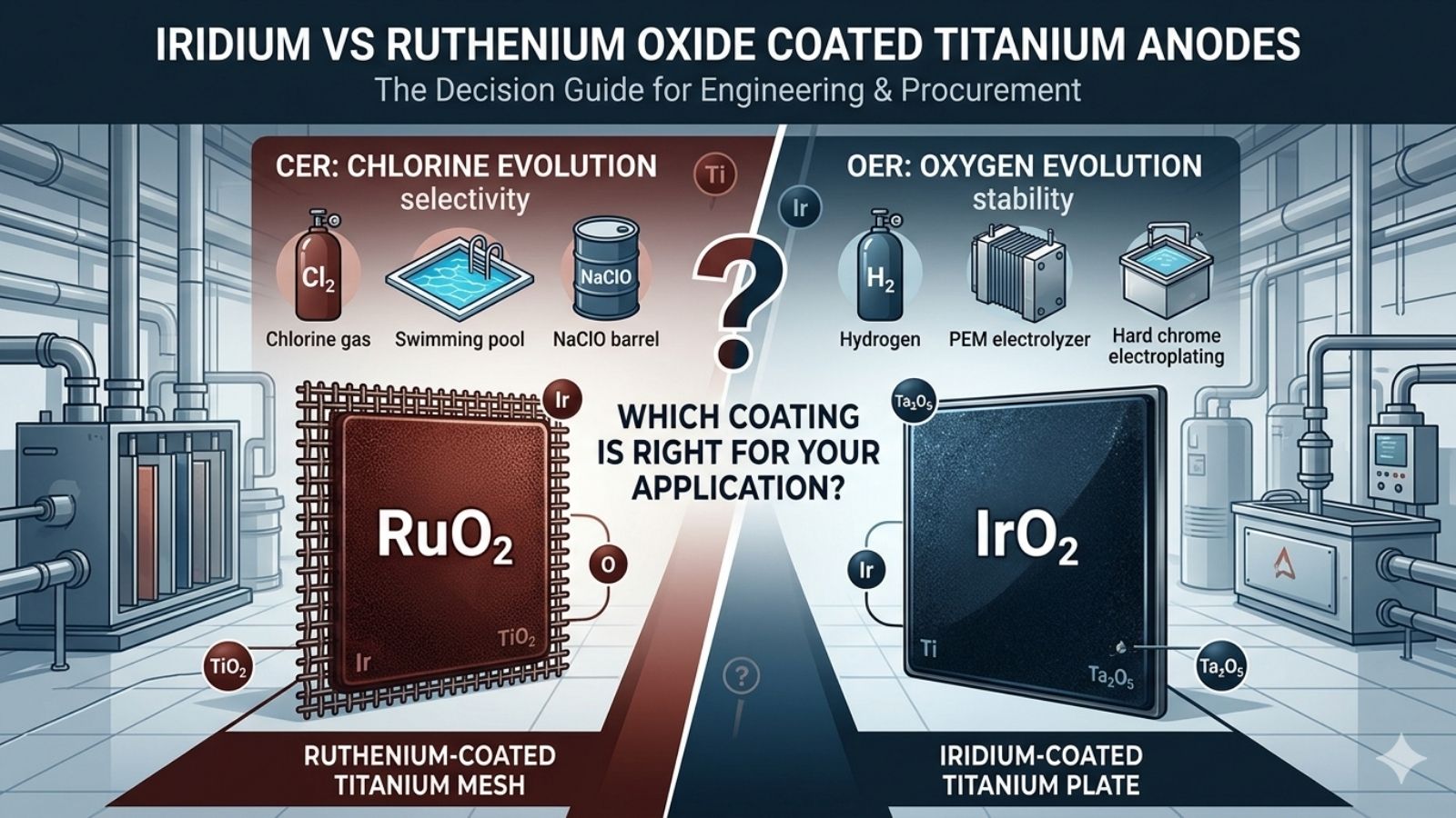 Apr 20, 2026Iridium Oxide vs Ruthenium Oxide Coated Titanium Anodes: Which Coating Is Right for Your Application?
 -
Mar 13, 2026Titanium Anode for PCB Gold Plating: Key Technologies for Uniform Coating
-
 Mar 13, 2026Titanium Anode Applications in Industrial Wastewater Treatment: Electrolytic Degradation
 -
 Mar 13, 2026Titanium Anode Technology for Swimming Pool Treatment: 3D Double-Layer Structure Advantages


Set A Consultation Today
Name can't be empty
Email error!
Send Your Message
*We respect your confidentiality and all
information are protected.
